Alumina, as a raw material for aluminum products and an auxiliary material in industries like chemicals and machinery, has long played an important role in the national economy. With the rapid development of emerging industries such as semiconductor, the demand for high-performance materials has surged. High-end alumina products have become crucial, especially in the trillion-dollar markets of semiconductor, where alumina is a key foundational material.
Semiconductor Market
As applications like AI, 5G communication, IoT, cloud computing, automotive electronics, robotics, and drones continue to grow, the semiconductor industry is booming.

According to several market research organizations, the global semiconductor market saw significant growth in 2024. For example, the World Semiconductor Trade Statistics (WSTS) reported that the global semiconductor market reached 45.76 trillion RMB in 2024, a 19% increase. The Chinese semiconductor market grew 20%, representing 30% of the global market. WSTS forecasts an 11.2% growth in 2025, reaching 697 billion USD. Deloitte also predicts 2025 sales of 697 billion USD and expects the semiconductor industry to hit 1 trillion USD in sales by 2030.
Alumina Applications in the Semiconductor Industry
Semiconductor Equipment Components
Alumina ceramic parts are known for their high hardness, mechanical strength, wear resistance, high temperature tolerance, electrical resistivity, and insulation properties. These features make them essential for semiconductor manufacturing in vacuum, high-temperature, and other special environments. Alumina plays an irreplaceable role in semiconductor production lines, covering nearly all semiconductor equipment and forming the core parts of the equipment.
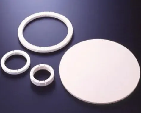
Alumina ceramic components are classified by their use, including ring and cylinder types, airflow guides, load-bearing fixtures, hand-held washers, and modules.
Ring and Cylinder Types: In the etching process, high-purity alumina coatings or ceramic parts are used for etching chambers and their liners. These materials are highly corrosion-resistant and reduce contamination during plasma etching.
Alumina Ceramic Components in Semiconductor Equipment
| Product Type | Function | Semiconductor Equipment Application |
| Molybdenum Ring | Enhances gas guidance, insulation, and corrosion resistance | Thin-film deposition equipment |
| Protection Ring | Protects key module components such as electrostatic chucks and ceramic heaters | Thin-film deposition equipment, etching equipment |
| Edge Ring | Prevents plasma overflow | Thin-film deposition equipment, etching equipment |
| Focus Ring | Concentrates plasma within the chamber | Thin-film deposition equipment, etching equipment, ion implantation equipment |
| Protective Cover | Seals and adsorbs process residues | Thin-film deposition equipment, etching equipment |
| Ground Clamp Ring | Secures and supports components | Thin-film deposition equipment, etching equipment |
| Liner | Enhances gas guidance for more uniform film formation | Etching equipment |
| Thermal Barrel | Improves temperature control performance | Thin-film deposition equipment, etching equipment, ion implantation equipment |
| Thermocouple Protection Tube | Protects thermocouples in a relatively stable temperature and physicochemical environment | Various semiconductor front-end equipment |
Gas Flow Guide Components
In the plasma cleaning process, corrosive gases containing highly reactive halogen elements like fluorine and chlorine are used. The gas nozzles are usually made from alumina ceramics, requiring high plasma resistance, dielectric strength, and strong corrosion resistance to the process gases and by-products. These nozzles also have precise internal pore structures to control the gas flow accurately.
Gas-guiding alumina ceramic components are mainly used in semiconductor equipment
| Product Type | Function | Semiconductor Equipment Application |
| Nozzle, Gas Distribution Plate, Restriction Ring, Diffuser Plate | Guides gas flow, ensures uniform distribution and stable velocity of process gases, and creates a controlled process environment | Thin-film deposition equipment, etching equipment |
| Nozzle Cover Plate | Serves as an attachment for nozzles and adsorbs process residues | Thin-film deposition equipment, etching equipment |
Load-bearing and Fixing Components
During semiconductor manufacturing, wafers may undergo high-temperature treatments like etching and ion implantation. Alumina wafer carriers are used to ensure the stability and safety of wafers during transportation. These carriers have excellent thermal conductivity, efficiently dissipating and directing heat away from the wafer to prevent thermal damage.
Hand-grip Washer Components
Alumina ceramic components are used in wafer handling, particularly in mechanical arms installed on wafer transfer robots. These arms act like the robot’s hands, moving wafers to specific positions, with their surfaces directly touching the wafers. Because wafers are extremely susceptible to contamination, the handling is usually performed in a vacuum environment. Most materials cannot withstand the conditions, so the mechanical arms are made from highly durable and high-hardness alumina ceramics. The ceramics are also precision-engineered with smooth surfaces, ensuring minimal contamination. Various designs are used, such as clamping, load-bearing, vacuum adsorption, and Bernoulli systems.
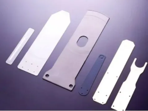
Alumina/Silicon Carbide Robotic Arms
Source: Kyocera, Japan
Hand-grip gasket-type alumina ceramic parts are mainly used in semiconductor equipment
| Product Type | Function | Semiconductor Equipment Application |
| Robotic Arm | Transfers wafers in and out of the chamber | Various semiconductor front-end equipment |
| Insulating Part | Prevents electrical conduction; some also provide insulation | Various semiconductor front-end equipment |
| Heat Sink | Cools equipment components | Various semiconductor front-end equipment |
Hand-grip Washer Components
Alumina ceramic components are used in semiconductor equipment, especially in module types. In deposition processes like Physical Vapor Deposition (PVD), Chemical Vapor Deposition (CVD), and Chemical Mechanical Polishing (CMP), components such as electrostatic chucks, ceramic heaters, polishing tables, polishing plates, chambers, and other parts are made from alumina ceramics.
High-purity alumina polishing plates are commonly used, sourced from Kyocera, Japan.
Ceramic Substrates
Ceramic substrates stand out due to their excellent insulation properties, high strength, low thermal expansion coefficient, and superb chemical stability and thermal conductivity. They are widely regarded for use in integrated circuit packaging.
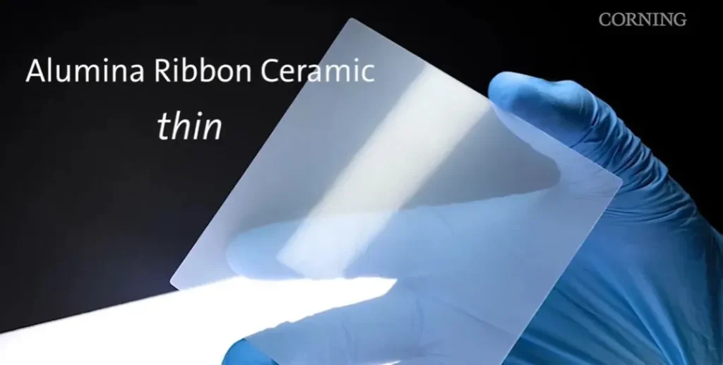
Corning has developed ultra-thin alumina ceramic substrates.
Alumina ceramic substrates are extensively used in RF and microwave electronics due to their high dielectric constant, enabling circuit miniaturization. They also exhibit excellent thermal stability, minimal temperature drift, high substrate strength, and chemical stability, outperforming most other oxide materials. These substrates are suitable for thick-film circuits, thin-film circuits, hybrid circuits, microwave component modules, and more. Alumina ceramic substrates are cost-effective (about 1/10 the price of aluminum nitride), with a mature production process, making them the most widely produced and used in the industry.
CMP Polishing Abrasives
Chemical Mechanical Polishing (CMP) is currently the only technology that can achieve global planarization and is widely used in semiconductor wafer polishing, shallow trench isolation, copper interconnects, and more.
Abrasives play a critical role in CMP by performing mechanical actions like micro-cutting and scratching. Polishing liquids account for 49% of the CMP polishing material cost, while abrasives contribute 50%-70% of the polishing liquid cost.
Source: Guangzhou Huifu Research Institute
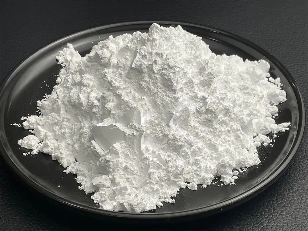
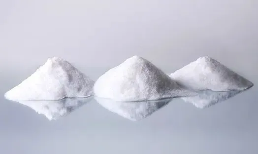
The most commonly used abrasives include SiO2, CeO2, and Al2O3. Among them, high-purity submicron spherical alumina powder, used as an abrasive in CMP polishing liquids, offers high removal rates, fast polishing, minimal fine scratches on the polished surface, and a high level of smoothness. It is ideal for use in the polishing process of semiconductors.
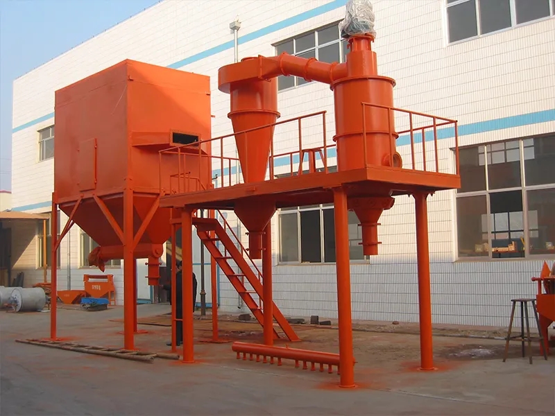
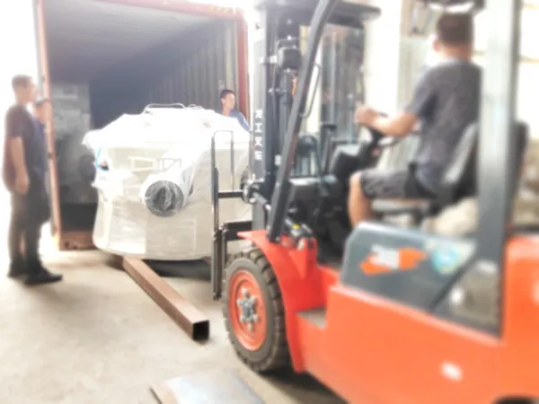
About Epic Powder Machinery
Epic Powder Machinery is a leading provider of advanced ultrafine grinding and air classification equipment. With over 20 years of experience in the field, our innovative solutions support industries like semiconductors, new energy, and pharmaceuticals. We are committed to delivering high-performance equipment and exceptional service to help our customers achieve the best results.
Explore our products and services to discover how we can assist you in optimizing your manufacturing processes.